Components Overview
A complete NE302 shipment includes the Main Board and Interface Board as a two-board platform. The Main Board contains the image, compute, memory, wireless, and control circuits; the Interface Board provides USB Type-C, MicroSD, programming, and service access. The Main Board can also be used in a custom Main-Board-only integration with DC power; this form does not use the MicroSD slot on the Interface Board. This page identifies those hardware blocks. For cable connection and firmware flashing, use Hardware Connection.
Main Board component map
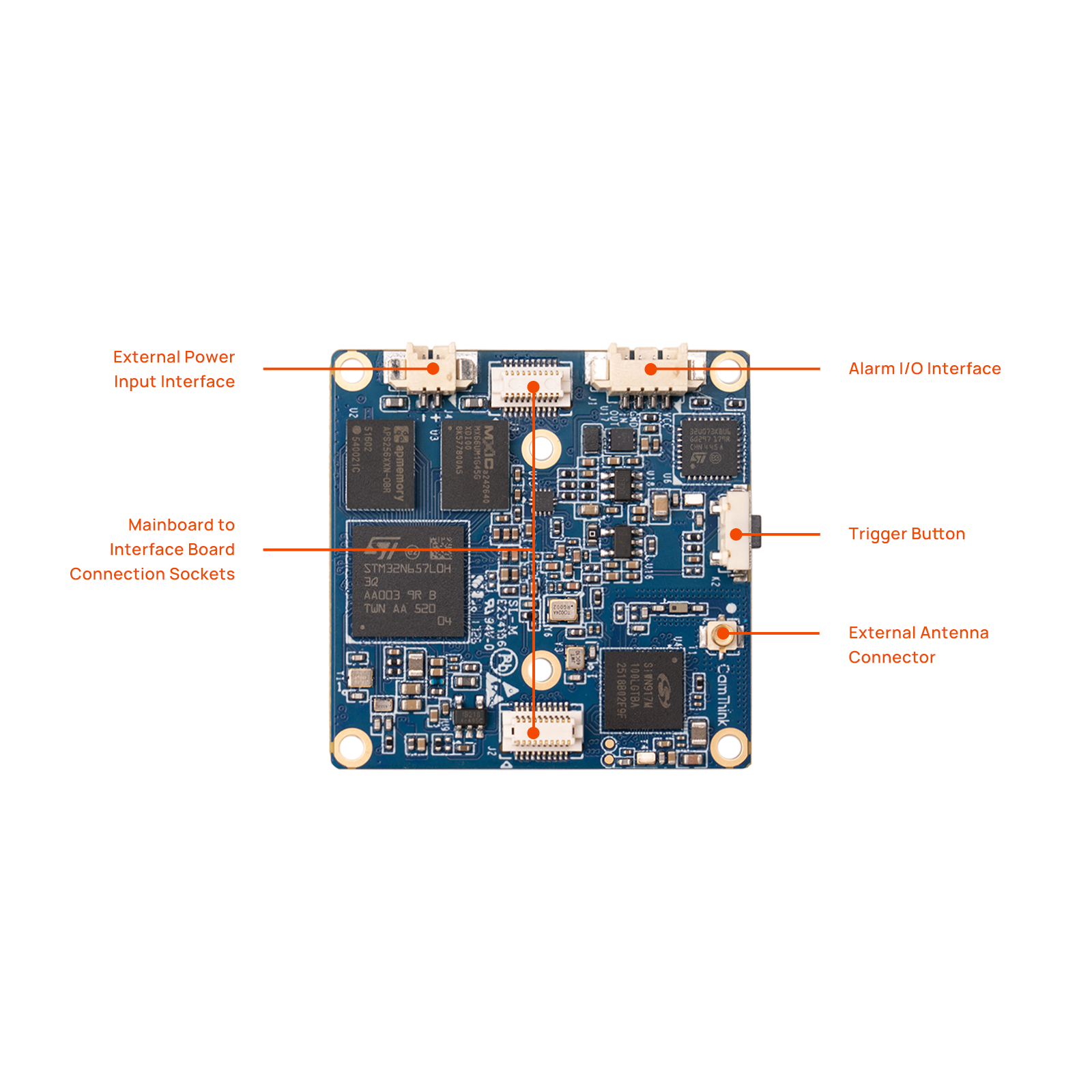
| Component | Circuit role | Connected hardware path |
|---|---|---|
| STM32N657L0H3 | Primary vision and AI MCU | Receives the camera stream and connects to PSRAM, Flash, Wi-Fi, and the Interface Board |
| STM32U073K8U6 | Low-power control MCU | Handles power-control and wake/control signals, including Trigger and Reset-related control paths |
| APS512XXN-OBR-BG PSRAM | 32 MB runtime memory | Connected to STM32N657 through the XSPIM P1 interface |
| OSPI Flash | 64 MB non-volatile storage | Connected to STM32N657 through the XSPIM P2 interface; firmware packages and partition addresses must match this hardware |
| SiWN917M100LGTBA | 2.4 GHz Wi-Fi 6 and Bluetooth wireless module | Connected to STM32N657 through the Wi-Fi SPI/control path and the fitted antenna connection |
| OS04C10-A43A | 4 MP CMOS image sensor | Uses the MIPI camera data path and I2C control path to STM32N657 |
| MP2410AGJ | White-LED driver | Drives the onboard illumination through the PWM_LED control path |
The Main Board also carries the external-power input, Alarm I/O, Trigger button, external-antenna connector, and board-to-board sockets shown in the component map. These labels identify the physical areas; they do not publish a field-wiring pinout or electrical limit.
Main Board rear and Reset
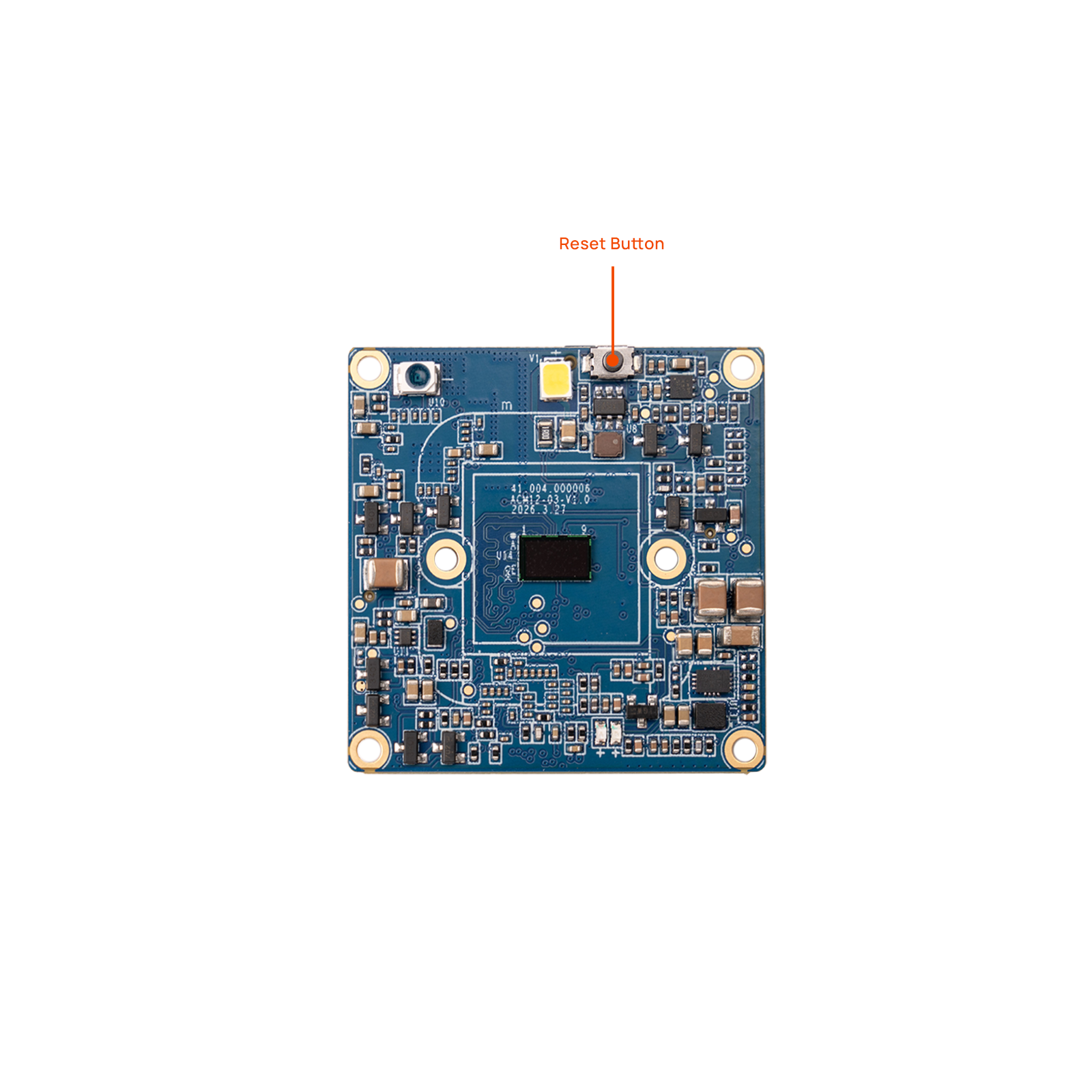
The rear-side map identifies the Reset Button. Use Reset only when the operating procedure requires it. It restarts the device; it is not a substitute for selecting the N6 or U0 programming target.
Imaging, compute, and control paths
STM32N6 and STM32U0 are separate MCUs. Before flashing, identify the target from the Interface Board silk-screen label; switch settings, ST-LINK wiring, and commands are in Build, Flash and Update.
Interface Board component map
The Interface Board includes the USB-C and MicroSD connection circuits, programming headers, and an SHT31-DIS temperature/humidity sensor. The component is present on the board, but the standard enclosure has no opening for it; it must not be presented as an enclosure-level ambient temperature/humidity measurement feature.
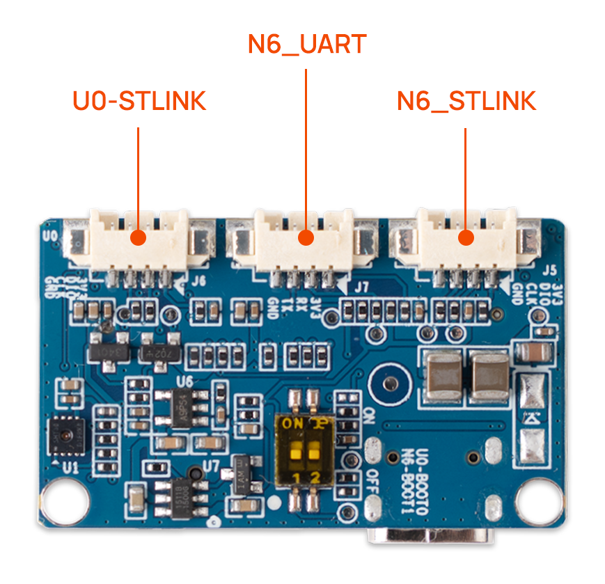
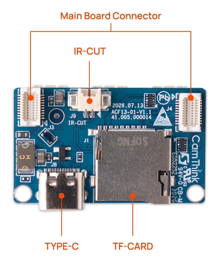
| Interface-board component or area | Function | Use boundary |
|---|---|---|
| USB-C circuit | Device power and USB connection | Use the approved USB-C supply and cable for the delivered unit |
| MicroSD circuit | Local card access | Follow the current device procedure; if hot-plug behavior is not explicitly supported, stop the device and disconnect power before handling the card |
| SHT31-DIS | Temperature/humidity sensor present in the schematic | The standard enclosure has no opening for the sensor, and its firmware read path and Web UI exposure were not verified; do not present it as an enclosure-level ambient measurement feature |
| IR-CUT connector | IR-cut filter switch control connector (labeled in the image) | Its control path and firmware support are not verified in this guide; follow the delivered documentation before wiring |
| N6_STLINK / U0-STLINK | Separate SWD programming paths | Select the path that matches the firmware target |
| N6_UART | STM32N6 serial-console connector | Use only with the matching adapter and serial procedure; the source README lists 921600 baud |
| N6-BOOT / U0-BOOT | Programming-mode controls | Change the matching switch only while the device is unpowered |
Related resources
- Board assembly, USB-C, MicroSD, N6_UART, and ST-LINK: Hardware Connection
- Build and flashing commands: Build, Flash and Update
- Schematics, PCB files, and project sources: NE302 source repository